
Description
Product Overview
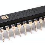
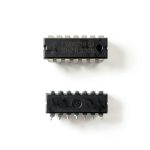
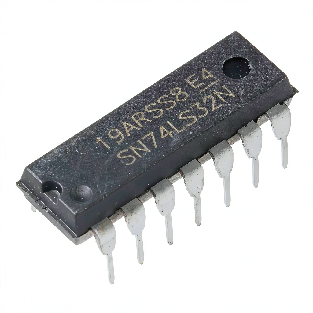
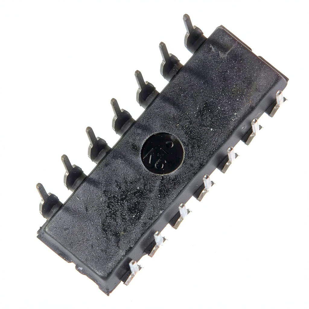
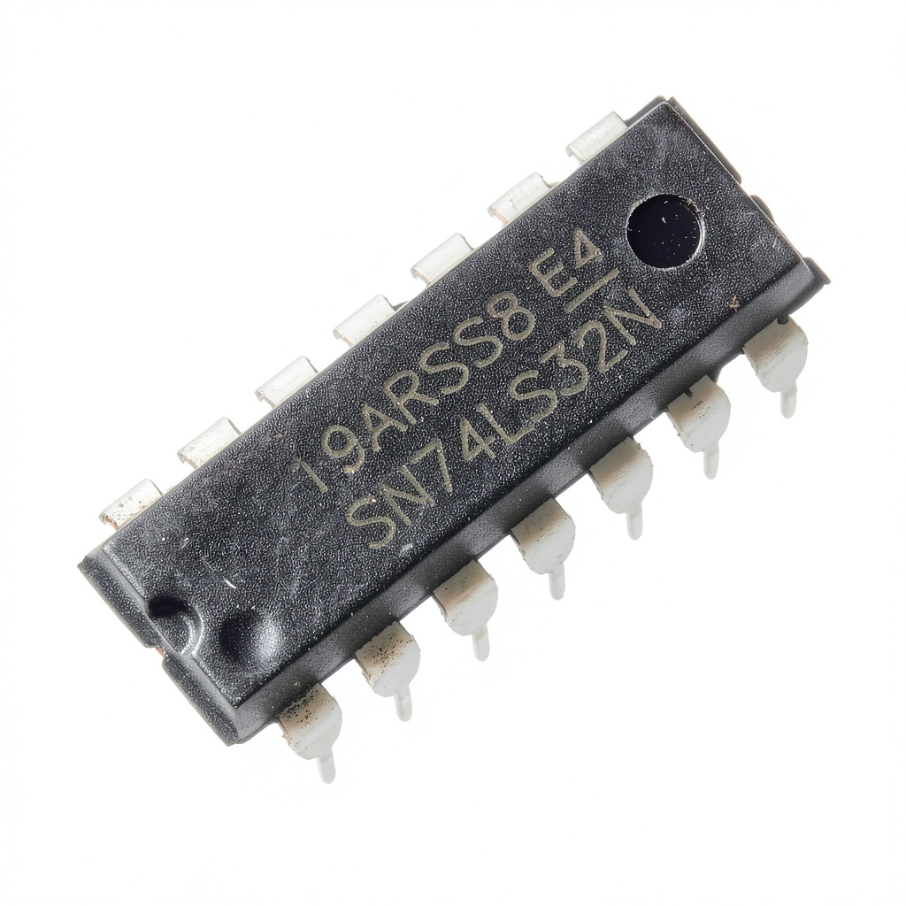
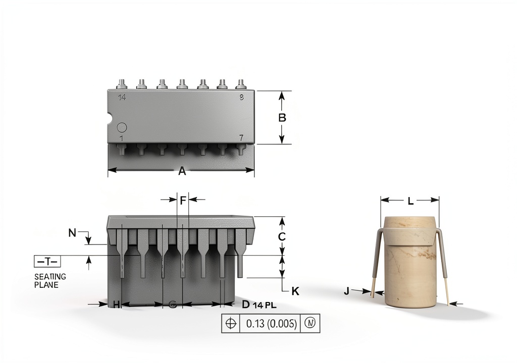
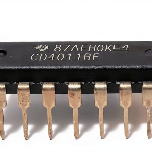
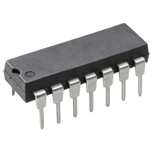
The SN74LS32N is a high‑performance quad 2‑input positive OR gate integrated circuit designed for a wide range of digital applications. Manufactured by Bridgold, this chip is housed in a standard 14‑pin DIP package that measures 5.04 x 2.68 x 0.31 inches and weighs only 0.63 ounces, making it easy to integrate into both compact and larger board layouts. Each unit provides four independent OR gates, each with a typical propagation delay of a few nanoseconds, ensuring rapid signal processing and minimal latency. The device operates from a 5 V supply and features TTL‑compatible input thresholds, allowing seamless interfacing with legacy logic families as well as modern CMOS circuits. With a robust silicon construction, the SN74LS32N tolerates a wide temperature range from –55 °C to +125 °C, making it suitable for harsh industrial environments. The 20‑piece bulk pack (model bg‑193) offers a cost‑effective solution for designers who need multiple units for prototyping, production runs, or educational labs. Bridgold’s reputation for reliable semiconductor manufacturing adds confidence that each chip meets stringent quality standards, as reflected in its consistent performance across thousands of units.
![[Product front view showing all components]](https://www.palvix.store/wp-content/uploads/2026/07/781a3a3c1d2f474b8c7342e128a785e6.jpg)
Usage
This versatile OR gate is ideal for a variety of applications, including industrial control systems, automation equipment, data acquisition modules, and educational teaching kits. Engineers often employ the SN74LS32N in combinational logic circuits, such as address decoding, multiplexing, and signal conditioning, where multiple input signals must be combined to generate a single output. Its fast switching capability makes it suitable for timing‑critical tasks like pulse‑width modulation and clock generation. In prototype environments, the DIP‑14 form factor simplifies breadboard testing and rapid iteration, while the 20‑piece quantity ensures that developers have enough units for iterative design cycles and verification. The chip’s low power consumption also benefits battery‑operated devices and portable instrumentation, extending operational life without sacrificing performance. Additionally, the device’s 3‑state output feature allows it to drive bus lines directly, providing flexibility in complex bus architectures and enabling efficient data flow control in multi‑device systems.
Why Choose Us
Choosing Bridgold’s SN74LS32N means selecting a component backed by decades of semiconductor expertise and a commitment to quality assurance. Each chip undergoes rigorous testing for electrical characteristics, temperature stability, and long‑term reliability, ensuring that it meets or exceeds industry specifications. Bridgold provides comprehensive technical documentation, including detailed pin‑out diagrams, timing charts, and application notes, which help engineers accelerate development and reduce time‑to‑market. Our responsive customer support team is available to assist with design queries, troubleshooting, and sourcing advice, offering a level of service that many generic distributors cannot match. Moreover, the bulk packaging reduces per‑unit cost, delivering economic value for large‑scale projects while maintaining the same high‑quality standards. With a proven track record in industrial and scientific markets, Bridgold’s components are trusted by OEMs, research institutions, and hobbyists alike, making the SN74LS32N a reliable choice for any digital logic requirement.
Key Features
- Four independent OR gates in a single DIP‑14 package, reducing board space and component count.
- Fast nanosecond‑scale switching ensures high‑speed signal processing for time‑critical applications.
- Low power consumption and wide temperature range support both portable devices and harsh industrial environments.
- TTL‑compatible inputs provide seamless integration with legacy and modern logic families.
- Comprehensive technical support and documentation from Bridgold guarantee smooth design and implementation.
FAQ
What is the maximum operating voltage for the SN74LS32N?
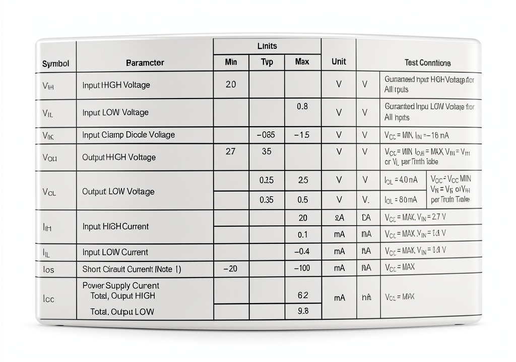
The device is specified for a supply voltage range of 4.5 V to 5.5 V, with a typical operating point of 5 V. Operating outside this range may affect switching speed and logic levels.
Can the SN74LS32N be used in low‑power battery‑operated projects?
Yes. The chip’s low quiescent current and efficient design make it suitable for battery‑powered applications where power conservation is critical, while still delivering reliable logic performance.
How does the 3‑state output feature benefit bus line driving?
The 3‑state (high‑impedance) output allows the gate to disconnect from a shared bus when not actively driving, preventing contention and enabling multiple devices to share the same communication line safely.
Is the SN74LS32N compatible with CMOS logic levels?
While the chip is TTL‑compatible, its input thresholds are compatible with many CMOS families operating at 5 V. Designers should verify voltage levels for specific CMOS devices to ensure proper logic interpretation.
What warranty or guarantee does Bridgold provide for this component?
Bridgold offers a standard limited warranty covering manufacturing defects for a period of one year from the date of purchase. Detailed warranty terms are available in the product documentation and can be confirmed with the supplier.

Reviews
There are no reviews yet.