
Description
Product Overview
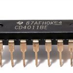
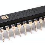
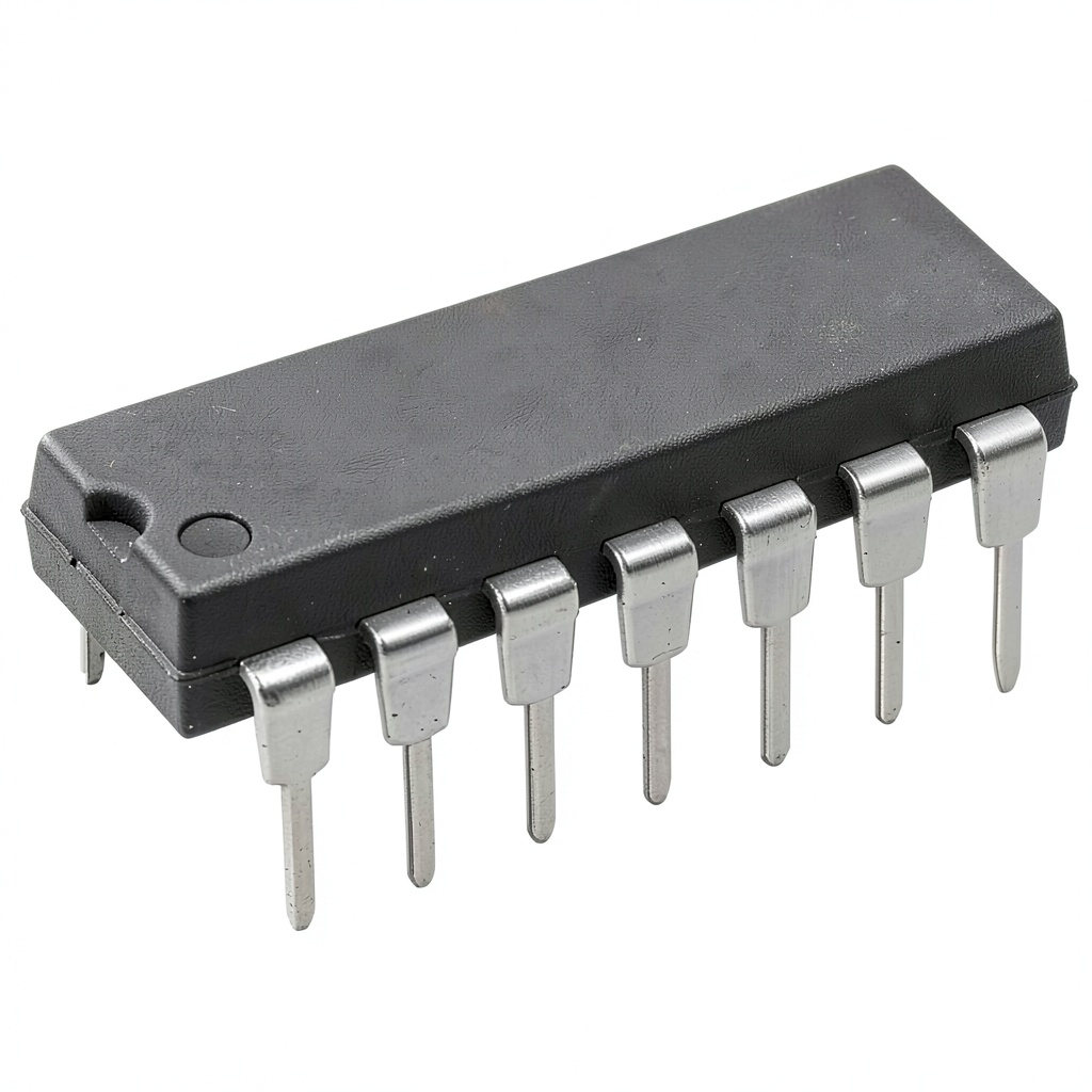
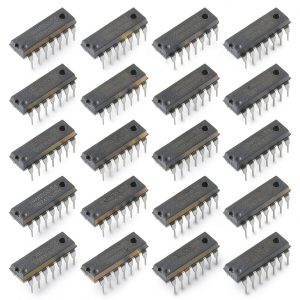
The 74LS10 Triple 3 Input Positive NAND Gate is a high‑performance logic device designed for demanding industrial and scientific environments. Manufactured by Major Brands, this component integrates three independent NAND gates, each accepting three inputs and delivering a positive logic output. Housed in a standard 14‑pin DIP (Dual In‑Line Package), the device occupies minimal board space while providing robust electrical characteristics that meet the LS (Low‑Power Schottky) family specifications. Its construction utilizes silicon semiconductor material with Schottky clamping diodes, resulting in reduced propagation delay and lower power dissipation compared with traditional TTL NAND gates. The 20‑pack offering ensures ample inventory for prototype development, small‑scale production runs, and maintenance stock, delivering cost‑effective reliability for engineers and system designers.
Key specifications of the 74LS10 include a typical propagation delay of 9 nanoseconds, a maximum fan‑out of 10 standard TTL loads, and a supply voltage range of 4.75 V to 5.25 V. The device operates with a low quiescent current, typically 10 mA per gate, which contributes to overall system efficiency. Electrical parameters such as input high voltage (VIH) of 2.0 V and input low voltage (VIL) of 0.8 V guarantee reliable switching thresholds, while the output high voltage (VOH) remains close to the supply rail, ensuring strong logic levels for downstream circuitry. The package dimensions of 8.94 × 0.59 × 0.55 inches and a weight of 0.67 ounces make the component easy to handle during manual assembly or automated pick‑and‑place processes.
Reliability is a cornerstone of the 74LS10 design, with each gate tested to meet industry‑standard temperature ranges from –55 °C to +125 °C. This broad operating envelope allows the component to function reliably in harsh environments such as automotive control units, industrial automation controllers, and laboratory instrumentation. The device’s built‑in Schottky diodes help to protect against voltage spikes and reduce latch‑up susceptibility, further enhancing durability. In addition, the 20‑pack configuration provides a convenient bulk solution for designers who require multiple gates across several boards, simplifying inventory management and reducing lead times.
From a design perspective, the 74LS10 offers flexibility in circuit topology. Its triple‑gate arrangement enables compact implementation of complex logic functions, such as building larger NAND structures, creating programmable logic arrays, or forming combinational networks for state machines. Engineers can cascade the gates to achieve higher input counts or integrate them with other LS‑family devices to maintain consistent timing characteristics across a system. The standard 14‑pin DIP footprint aligns with common breadboard and prototype board layouts, facilitating rapid testing and iteration without the need for specialized adapters.
Manufacturing processes for the 74LS10 incorporate advanced photolithography and precision doping techniques to achieve consistent transistor characteristics across the entire wafer. The result is a uniform threshold voltage and switching behavior that simplifies timing analysis in multi‑gate designs. Additionally, the device’s lead‑frame is engineered for optimal thermal conductivity, allowing efficient heat dissipation during high‑frequency operation. This attention to detail in both silicon and package engineering ensures that the component performs reliably even when subjected to rapid toggling in demanding digital circuits.
The 74LS10’s pin configuration follows the standard 14‑pin DIP layout, with pins 1‑7 and 8‑14 mirroring each other for the three NAND gates. This symmetry simplifies wiring on breadboards and printed circuit boards, reducing the chance of wiring errors. Detailed pinout diagrams and recommended wiring schematics are available in the product datasheet, providing engineers with clear guidance for integrating the gates into larger logic networks. Compatibility with other LS‑family devices such as the 74LS00 and 74LS02 further enhances design flexibility, allowing mixed‑family solutions without compromising timing consistency.
Usage
In practical applications, the 74LS10 is frequently employed in digital control systems where multiple logical conditions must be evaluated simultaneously. For example, in a motor control unit, three sensor signals can be combined using a single NAND gate to generate a safety shutdown command when any abnormal condition is detected. The triple‑gate configuration allows designers to implement three independent safety checks within a single IC, reducing board space and component count while preserving clear signal routing.
Another common use case is in data acquisition systems where multiple analog‑to‑digital converters (ADCs) require synchronized enable signals. By feeding the enable lines into one of the NAND gates, the 74LS10 can ensure that all converters are activated only when a master control signal is high, preventing unintended sampling. This coordinated control improves measurement accuracy and reduces noise introduced by unsynchronized converter operation.
The 74LS10 also finds application in educational labs and hobbyist projects where students experiment with Boolean logic and truth tables. Its clear pinout and reliable switching make it an ideal teaching tool for demonstrating how NAND gates can be combined to create any other logic function. Because the device operates at standard TTL voltage levels, it can be directly interfaced with popular microcontroller platforms such as Arduino or Raspberry Pi, enabling hands‑on learning without additional level‑shifting circuitry.
In high‑speed data communication modules, the 74LS10 can be employed to generate control signals that synchronize data lanes. By using one NAND gate to create a clock enable and another to monitor error flags, designers can build a compact supervisory circuit that quickly disables transmission upon fault detection, protecting downstream components from damage. The fast switching speed of the LS family ensures that these control signals keep pace with modern gigabit data rates, making the 74LS10 a viable choice for both legacy and contemporary communication standards.
For hobbyist robotics projects, the 74LS10 can serve as a central decision‑making unit that processes multiple sensor inputs to drive motor control logic. For instance, proximity, temperature, and voltage sensors can each feed into separate inputs of a NAND gate, producing a single output that commands a motor driver only when all safety thresholds are satisfied. This logical consolidation reduces the need for multiple discrete components, simplifying the wiring harness and freeing up valuable board real estate for additional functionality such as wireless communication modules.
Why Choose Us
Choosing the 74LS10 from Major Brands guarantees a product that adheres to rigorous quality standards throughout its manufacturing lifecycle. Each IC undergoes comprehensive testing for electrical performance, thermal stability, and long‑term reliability, ensuring that the gates meet or exceed the specifications defined by the LS logic family. The company’s commitment to traceability means that every batch can be traced back to its production lot, providing confidence for critical applications where component provenance is essential.
In addition to the core performance benefits, the 20‑pack supply format offers logistical advantages for manufacturers and repair technicians. Bulk packaging reduces the number of individual shipments, lowering handling costs and minimizing the risk of lost or misplaced components. The consistent packaging also simplifies inventory management, allowing stockrooms to maintain a single SKU for multiple design projects, which streamlines ordering processes and improves lead‑time predictability.
Major Brands provides dedicated technical support and after‑sales service for the 74LS10 series. Customers can access detailed datasheets, application notes, and reference designs through the company’s online portal, facilitating rapid integration into new projects. Should any issues arise, the support team offers troubleshooting assistance and warranty coverage, reinforcing the reliability of the component throughout its operational lifespan.
The reliability of the 74LS10 is further reinforced by its compliance with RoHS (Restriction of Hazardous Substances) directives, ensuring that the component is free from lead and other hazardous materials. This environmental compliance is increasingly important for manufacturers seeking to meet global sustainability standards and for end‑users who require eco‑friendly components in their products. By selecting a RoHS‑compliant part, designers can avoid regulatory hurdles and streamline certification processes.
Major Brands also offers a comprehensive warranty program that covers manufacturing defects for a period of two years from the date of purchase. This warranty, combined with a responsive technical support hotline, provides customers with confidence that any unexpected issues will be addressed promptly. The company’s extensive distribution network ensures that replacement units are readily available, minimizing downtime for critical applications.
Key Features
- Three independent NAND gates each with three inputs, enabling compact multi‑logic implementations and reducing board space.
- Low‑power Schottky design delivers typical propagation delay of 9 ns while keeping power consumption under 10 mA per gate.
- Wide operating voltage range of 4.75 V to 5.25 V ensures reliable performance across diverse power supplies.
- Robust temperature tolerance from –55 °C to +125 °C makes it suitable for harsh industrial and automotive environments.
- Comes in a 20‑pack bulk quantity with full technical support and warranty, simplifying inventory and providing peace of mind.
FAQ
What is the maximum fan‑out for the 74LS10 NAND gates?
The 74LS10 is designed to drive up to ten standard TTL loads per gate, which is the typical fan‑out rating for LS‑family devices. This means each output can reliably feed ten inputs of other TTL or LS logic chips without degradation of signal integrity. If the downstream circuitry includes higher‑capacitance loads or long trace lengths, the effective fan‑out may be reduced, and designers should consider adding a buffer or shortening the interconnects. The device’s low output impedance helps maintain fast rise and fall times even at the maximum fan‑out, ensuring that timing margins remain within specification. For applications that require driving more than ten loads, it is advisable to cascade additional NAND gates or use dedicated line drivers to preserve performance.
Can the 74LS10 be used with 3.3 V logic levels?
The 74LS10 is specified for a supply voltage range of 4.75 V to 5.25 V, which aligns with standard 5 V TTL logic. Operating the device at 3.3 V is outside its guaranteed specifications and can lead to undefined logic thresholds, reduced noise margins, and unreliable switching. However, some designers have successfully used LS‑family parts at lower voltages by carefully evaluating the VIH and VIL levels, which for the 74LS10 are 2.0 V and 0.8 V respectively. At 3.3 V supply, the high‑level input threshold may be marginally met, but the low‑level threshold could be too close to the supply rail, increasing the risk of false triggering. For robust 3.3 V designs, it is recommended to select a logic family specifically rated for that voltage, such as the 74HCT or 74LVC series, to ensure proper operation and compatibility with modern microcontrollers.
How does the 20‑pack packaging benefit large‑scale production?
Purchasing the 74LS10 in a 20‑pack configuration provides several practical advantages for manufacturers that require high volumes of logic components. First, bulk packaging reduces the per‑unit cost by minimizing packaging material and handling fees, which translates into lower overall bill of materials for the final product. Second, having twenty identical devices on a single reel simplifies automated pick‑and‑place programming, as the machine can feed the same part continuously without frequent reel changes, improving line efficiency and reducing downtime. Third, inventory management becomes more straightforward because a single SKU covers multiple design revisions, allowing engineers to stock a consistent part number across different projects. Finally, the larger quantity ensures that spare parts are readily available for field repairs, extending product support life and enhancing customer satisfaction.
What are the recommended PCB layout guidelines for minimizing noise?
To achieve optimal performance with the 74LS10, careful PCB layout is essential. Keep the input and output traces as short as possible to reduce parasitic capacitance and inductance, which can degrade switching speed. Route power and ground planes directly beneath the IC to provide a low‑impedance return path and improve thermal dissipation. Separate analog and digital sections of the board, and place decoupling capacitors (0.1 µF) close to the VCC pin of each gate to filter high‑frequency noise. Avoid running high‑current traces parallel to the logic signal lines, and use proper spacing between adjacent signal tracks to prevent crosstalk. Finally, follow the manufacturer’s recommended pin‑to‑pin spacing and maintain consistent trace widths to ensure uniform impedance throughout the circuit.
Is the 74LS10 compatible with other LS‑family logic devices?
The 74LS10 is fully compatible with other members of the LS logic family, such as the 74LS00 quad 2‑input NAND, 74LS02 quad 2‑input NOR, and 74LS04 hex inverter. All LS devices share the same supply voltage range, input threshold levels, and output drive characteristics, allowing them to be mixed on the same board without introducing timing mismatches. This compatibility simplifies the design of mixed‑logic circuits, as engineers can combine different gate types to implement complex Boolean functions while maintaining consistent propagation delays. When interfacing LS devices with newer logic families, it is advisable to verify that the voltage levels are within the acceptable range, but within the LS family the inter‑device compatibility is guaranteed by the standard specifications.
Overall, the 74LS10 Triple 3 Input Positive NAND Gate delivers a blend of performance, reliability, and flexibility that makes it a go‑to choice for engineers seeking proven logic solutions in demanding applications.
 MCP2004A-E/SN SOIC-8 NAND Logic Gate by Oyhrwt Compact 0.39" Package
 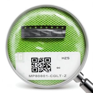 MP86901 CGLT Z NAND Logic Gate 2Pcs by CG Chips Gate Industrial
  Alternative Dispute Resolution eBook Good Books 2nd Ed Typesetting
  Pedophilia & Empire Kindle Edition by Joachim Hagopian Read eBook
  Two Hour Politics Short Read Skyhorse Kindle eBook Enhanced
Reviews
There are no reviews yet.